RISC-V · 55 nm · OSOC · Turin Polytechnic University in Tashkent
A RISC-V Microcontroller with a Custom PWM Engine
At Turin Polytechnic University in Tashkent, we have designed a RISC-V microcontroller with a custom pulse-width modulation (PWM) engine and submitted it for fabrication in a 55 nm CMOS process. The chip is aimed at low-power IoT devices and digitally controlled power electronics. To our knowledge, it is the first customized microcontroller designed in Uzbekistan to go into fabrication. The chips are expected in early 2027.

The design
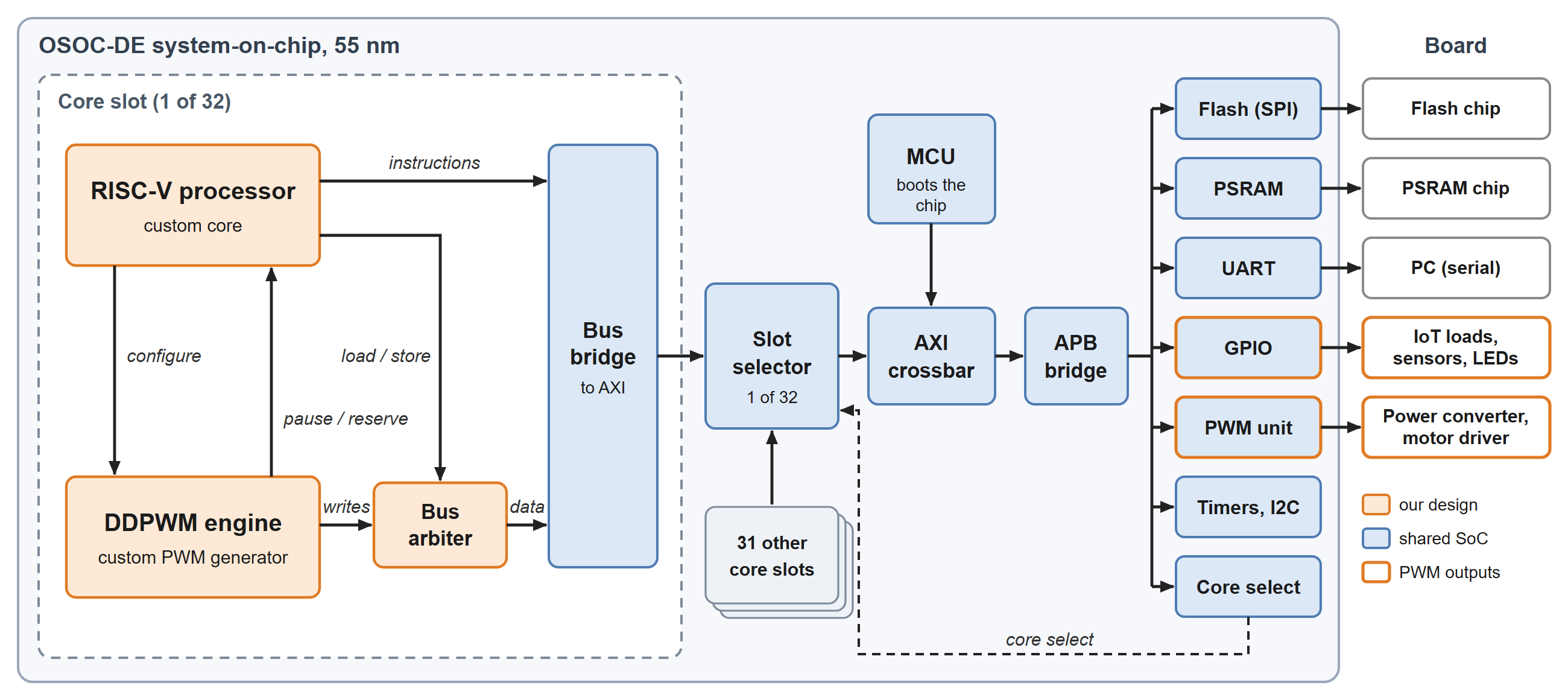
Our design has two parts: a RISC-V processor core and a hardware PWM engine built next to it (Fig. 1). We wrote both from scratch in Verilog. The processor runs C programs compiled with the standard RISC-V GCC toolchain. The engine produces the switching signal for a power converter, a motor driver or an LED driver. Once the processor has configured it, the engine runs on its own, period after period, and the processor only updates the duty cycle when the control loop needs it.
The design sits in one of the 32 core slots of OSOC-DE, a shared 55 nm system-on-chip. The chip supplies the memory and peripherals: SPI flash for the boot code, PSRAM for programs, a UART console, GPIO pins, a four-channel PWM unit, timers and I2C. A small management MCU boots the chip and selects the active slot. With our slot selected, the chip becomes a complete microcontroller built around our core and our PWM engine.
The PWM engine
Digitally controlled DC-DC converters need fine PWM resolution. If the resolution is too coarse, the output voltage can fall into limit cycles: small, persistent oscillations that the control loop cannot remove. A conventional digital PWM gains one bit of resolution only by doubling its clock frequency, and a faster clock costs power.
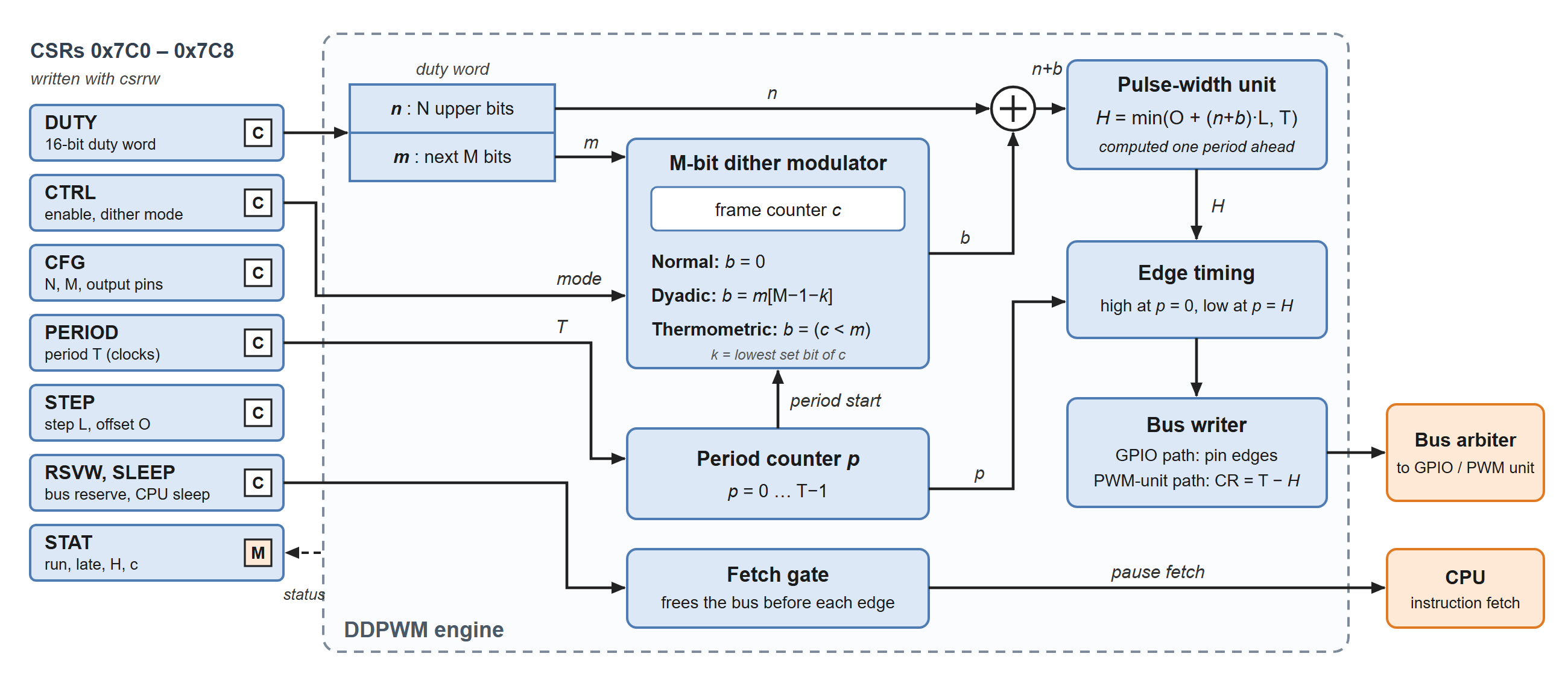
Our engine implements dyadic digital PWM (DDPWM), proposed by Crovetti, Usmonov, Musolino and Gregoretti [1]. The duty-cycle word is split into N coarse bits n and M fine bits m. In every switching period the pulse is n or n + 1 steps wide. A dither modulator sets the extra bit b so that, over a frame of 2^M periods, the average pulse width equals the full N + M-bit value. In [1], a buck converter switching at 100 kHz with a 5-bit digital PWM clocked at 3.2 MHz showed 46 mV limit cycles. DDPWM with N = 5 and M = 4, at the same 3.2 MHz clock, was free of them. A conventional 9-bit PWM would need a 51 MHz clock for the same resolution.
Fig. 2 shows how we built the method into hardware. The processor configures the engine through nine custom control and status registers (CSRs 0x7C0–0x7C8). N can be set from 2 to 12 and M from 0 to 8, and the dither modulator has three modes: normal (no dithering), dyadic, as in [1], and thermometric. A shift-add multiplier computes each pulse width one period in advance. Because the engine shares the bus with the processor, a fetch gate holds back instruction fetches just before each switching edge, so the engine's write always lands on time. The processor can also sleep for a chosen number of periods, which keeps the bus free while the engine runs.
From design to silicon
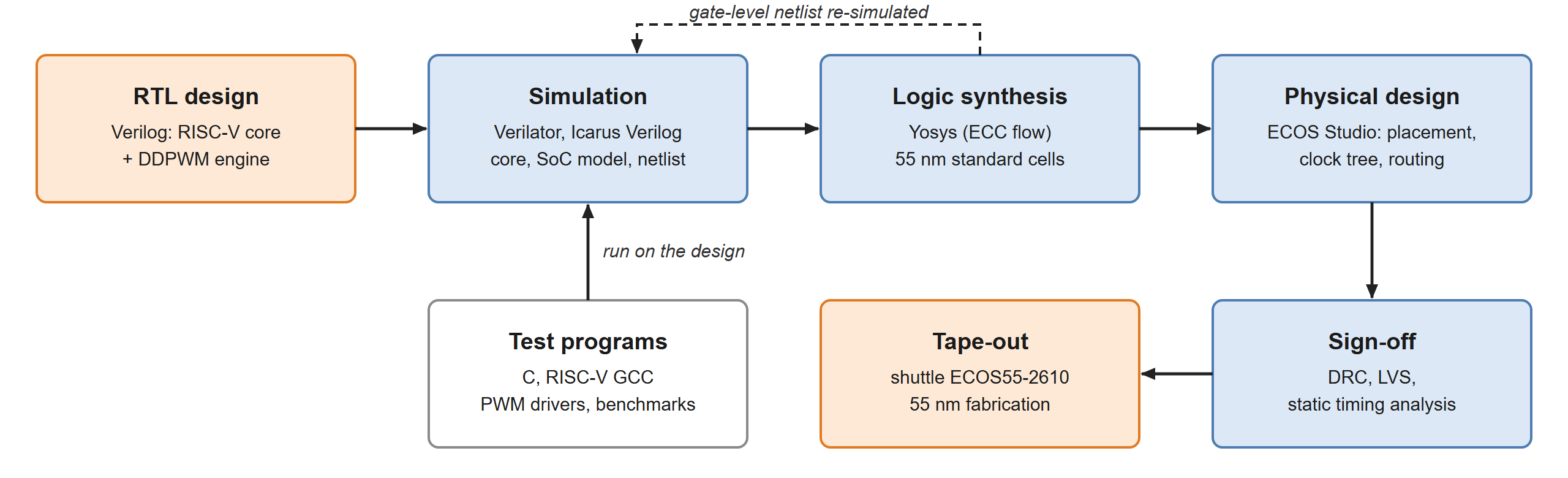
We verified the design at three levels with Verilator and Icarus Verilog: the core alone, the core inside a simulation model of the full chip, and the gate-level netlist after synthesis. C test programs exercised the instructions, the PWM engine and the real boot sequence of the shared chip. Yosys then mapped the design to 55 nm standard cells, and ECOS Studio placed and routed it (Fig. 3). The final layout has about 7,450 cells, 1,560 of them flip-flops, on a 214.6 × 215.4 µm die. It passed all 31 sign-off checks, including design-rule checks, layout-versus-schematic comparison and static timing analysis.
How it started
This project began at the Chip Design Bootcamp at Nazarbayev University in Astana (17–30 August 2026), organized by Prof. Nursultan Kabylkas, as part of One Student One Chip (OSOC), a program in which students design a processor from scratch and carry it through to fabrication. We finished the core at Turin Polytechnic University in Tashkent and, together with Maksud Usmonov, extended it with the PWM engine.
What comes next
The design was submitted through the OSOC program to the ECOS55-2610 shuttle, in which many designs share one silicon wafer, and is now in the manufacturer's review. The chips are expected in early 2027. When they arrive, we will bring up the microcontroller on a test board, run programs on it, and test the PWM engine in a working DC-DC converter.
Acknowledgements
We thank Maksud Usmonov of Turin Polytechnic University in Tashkent for his supervision and for proposing the PWM engine; Prof. Nursultan Kabylkas for the chip design bootcamp at Nazarbayev University in Astana; Prof. Zihao Yu and the One Student One Chip team for the course and for making the tape-out possible; and the ECOS team for the design tools and the shuttle.
References
[1] P. S. Crovetti, M. Usmonov, F. Musolino and F. Gregoretti, "Limit-cycle-free digitally controlled DC–DC converters based on dyadic digital PWM," IEEE Transactions on Power Electronics, vol. 35, no. 10, pp. 11155–11166, Oct. 2020.